
Introduction
Today I’m bringing you the disassembly, teardown, and analysis of a vintage Nokia d-box Multimedia Terminal (DVB) — a relic from the early days of digital broadcasting. This receiver teardown will reveal the inside of this classic device.
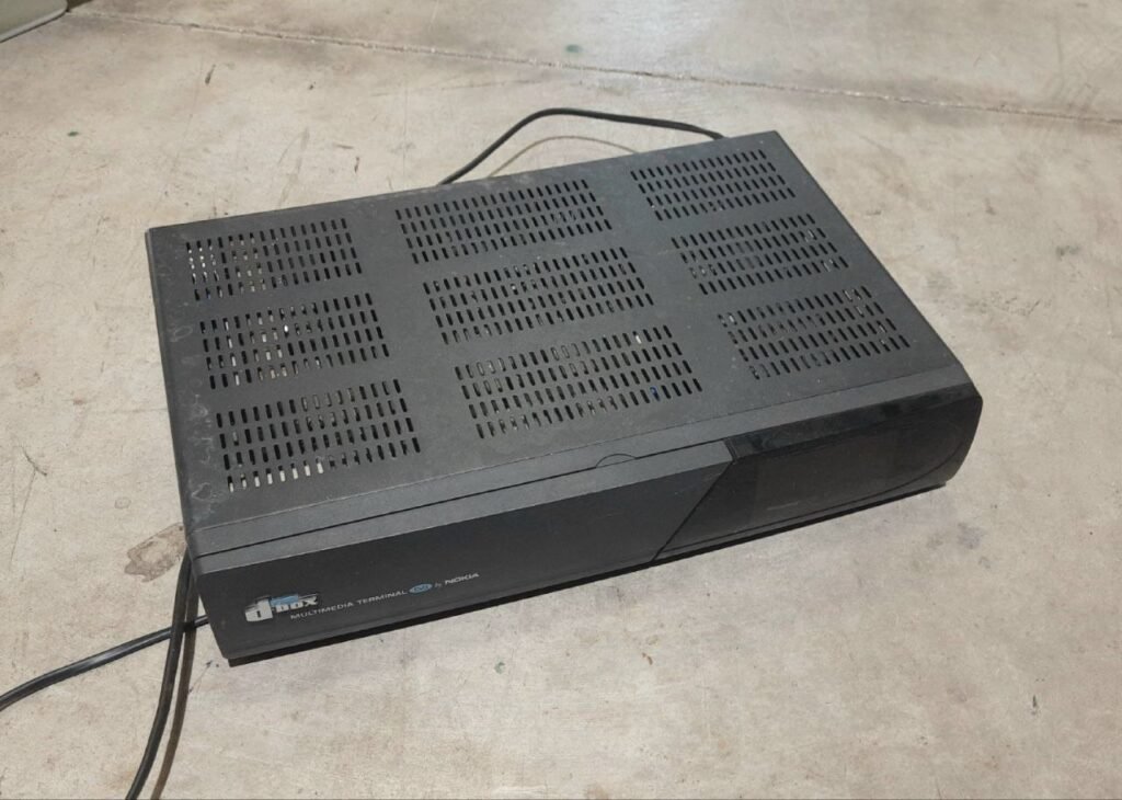
Background
Back in the day, these pay-per-view terminals were everywhere. Satellite and cable TV were at their peak, and streaming platforms like Netflix or Disney+ didn’t even exist yet. If you wanted premium content, you needed one of these boxes — often provided by your cable company — and a subscription card.
Teardown
Since this was high end stuff at the moment, i thought that it would probably house some interesting electronic components.
When I first tried to open the unit, I noticed it used security Torx screws on the top cover. I didn’t have the right bit at the moment, so I took it home to try again.
Later, I realized it wasn’t Torx at all — it was some kind of pentalobe security screw, the kind you rarely see outside of Apple devices. My iFixit kit didn’t include that bit either, so I had to resort to an extraordinary method to remove the cover. Let’s just say it wasn’t elegant, but it worked.
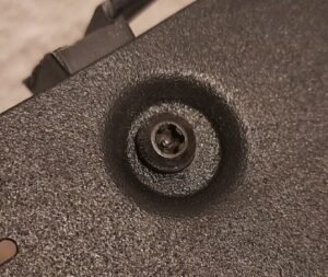
Security screw found in the Nokia d-box satellite receiver
The Nokia d-box DV3 is surprisingly well-built for a consumer-grade multimedia terminal. It features a plastic bottom shell where the main PCB is mounted, a metal top cover, a separate front panel, and a metal shield on the rear. Inside, there’s also a metal internal frame that adds rigidity and structural integrity once the unit is fully assembled.
To disassemble it, you’ll need a special pentalobe security screwdriver — not something you’ll find in a standard toolkit. Using unusual fasteners was common at the time, and many satellite and cable receivers of the era used similar anti‑tamper measures. Manufacturers weren’t only trying to discourage casual repairs; they were also responding to a growing wave of hardware experimentation. In the analog pay‑TV scene, for example, researchers often used popular video‑processing chips to analyze scrambled signals and study how the image was segmented or manipulated. With this kind of tinkering becoming widespread, especially in pay‑per‑view systems, adding physical barriers like security screws was one of the simplest ways to protect the internals and limit unauthorized access to premium content.
Main Board and Architecture
Let’s get into detail! What I was excited about those vintage receivers of the late 90’s is that they were very expensive so probably they would have a lot of electronic components is to see what kind of integrated circuits inside, memories, microcontrollers, maybe even an FPGA?
The receiver features a single main board with all elements integrated together on it (Power Supply, receiver and modem), although separated in different functional blocks. All of them are integrated except the control panel display, which is a commercial unit from Hyundai.
Power supply
The Nokia d-box DV3 uses a switching power supply that’s built directly into the main board rather than being handled by a separate PSU module. The 220 V AC mains feed enters straight onto the PCB, where the high‑voltage section takes care of converting alternating current into the various DC rails required by the digital electronics. Even though it’s part of the same board, the power-supply area is clearly isolated with wide clearance zones, silkscreen warning symbols, and dedicated component spacing — all intentional design choices meant to keep technicians from accidentally touching the high‑voltage section while the unit is powered.
One of the key components is the L4940D2T5, a 5V linear voltage regulator. It supplies power to the digital logic circuitry, but it’s likely that other parts — such as the display, modem, or RF receiver — require additional voltages.
Interestingly, I couldn’t locate a dedicated PWM controller IC, which is unusual. A switching power supply typically relies on a PWM chip to regulate voltage efficiently. It’s possible that the PWM functionality is embedded in another component or handled by a custom ASIC, but it’s definitely something worth investigating further.
Satellite Receiver
A separate, self‑contained tuner module, connected to the main board via a multi‑pin header. The entire unit is enclosed in a metal RF shield, both to reduce electromagnetic interference and to prevent stray signals from affecting the sensitive front‑end circuitry. This shielding also keeps the tuner’s local oscillators and intermediate‑frequency stages from radiating noise into the rest of the system, ensuring stable reception and compliance with regulatory emission limits.
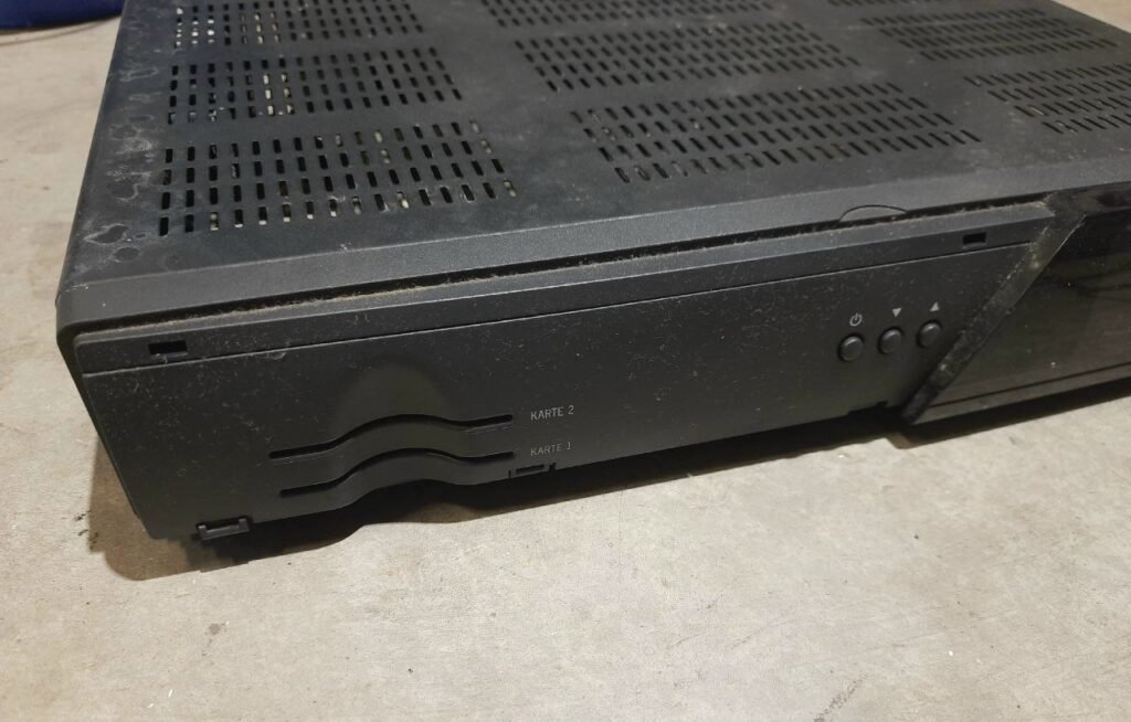
Modem
The Nokia d-box DV3 also incorporates a modem-related circuit on its main board. Although the television signal was received via satellite, the modem could provide a return channel over the telephone network, allowing the receiver to communicate with the service provider. This was particularly useful for interactive pay-TV services, such as pay-per-view ordering and subscription or billing management, since a satellite dish alone could receive broadcasts but could not transmit information back to the broadcaster.
Main Board
The main PCB carries the marking 5511985-03A in the copper layer and 55 11985-03 in the silkscreen, with the latter appearing on both the top and bottom sides of the board. The same Nokia d-box model may have been produced with different PCB revisions, so these board markings provide useful identification references when documenting the hardware or comparing boards from the same equipment family.
PCB Technology
The main board is a four-layer PCB with a standard thickness of 1.6 mm. It uses predominantly surface-mount technology (SMT), with components mounted on both sides of the board. Components on the bottom (solder) side were soldered using conventional wave soldering, not selective soldering. The smaller surface-mount components include 0805 packages, which have nominal body dimensions of approximately 2.0 × 1.25 mm.
The assembly combines top-side reflow soldering with bottom-side wave soldering. This mixed-technology process allows surface-mount devices and through-hole components to coexist on the same PCB without requiring a separate board for each assembly method.
The manufacturing sequence is as follows:
- Solder paste printing: Solder paste is deposited onto the top-side PCB pads through a stencil.
- Top-side component placement: A pick-and-place machine positions the surface-mount components onto the solder paste.
- Reflow soldering: The board passes through an infrared or convection reflow oven. The solder paste melts and forms the electrical and mechanical connections between the components and the PCB pads.
- Bottom-side component attachment: The board is prepared for assembly on the opposite side. Components intended for wave soldering are positioned on the bottom side and held in place with adhesive before the board is turned over. Red adhesive—usually Loctite SMD adhesive—is used for this purpose.
- Through-hole component insertion: Through-hole technology (THT) components are inserted into their plated holes before the wave-soldering stage. Radial and axial components can be inserted automatically using dedicated component-insertion machines.
- Wave soldering: The underside of the board passes over a controlled wave of molten solder. This solders the through-hole component leads and, where the design permits, the bottom-side surface-mount components. This board was not soldered using selective soldering.
When I first learned about electronics manufacturing, I was surprised to discover that surface-mount components can also be soldered by wave soldering, but this is an established assembly technique. The PCB layout must account for the direction of travel through the solder wave, component spacing, pad geometry and the risk of solder bridging. Component orientation is particularly important for small passive devices, as their geometry and the flow of molten solder can cause defects such as solder bridges or tombstoning. Solder thief pads can also be incorporated at the end of a row of pads to draw excess solder away from critical joints and help reduce bridging.
This approach makes it possible to assemble components on both sides of a PCB while combining reflow and wave-soldering processes
Display
As already stated, the display is a discrete separate module. It is manufactured by Hyundai, marked as HT12538-D on the PCB and HT12538FB-LYPF-04, which is likely an assembly or batch number. I haven’t seen the display working yet, since I haven’t powered up the receiver. However, it appears to be an LCD dot matrix display. Searching those part numbers only returns results related to the d-box itself, which suggests that the display was manufactured specifically for this device.

Close picture of the display. Source